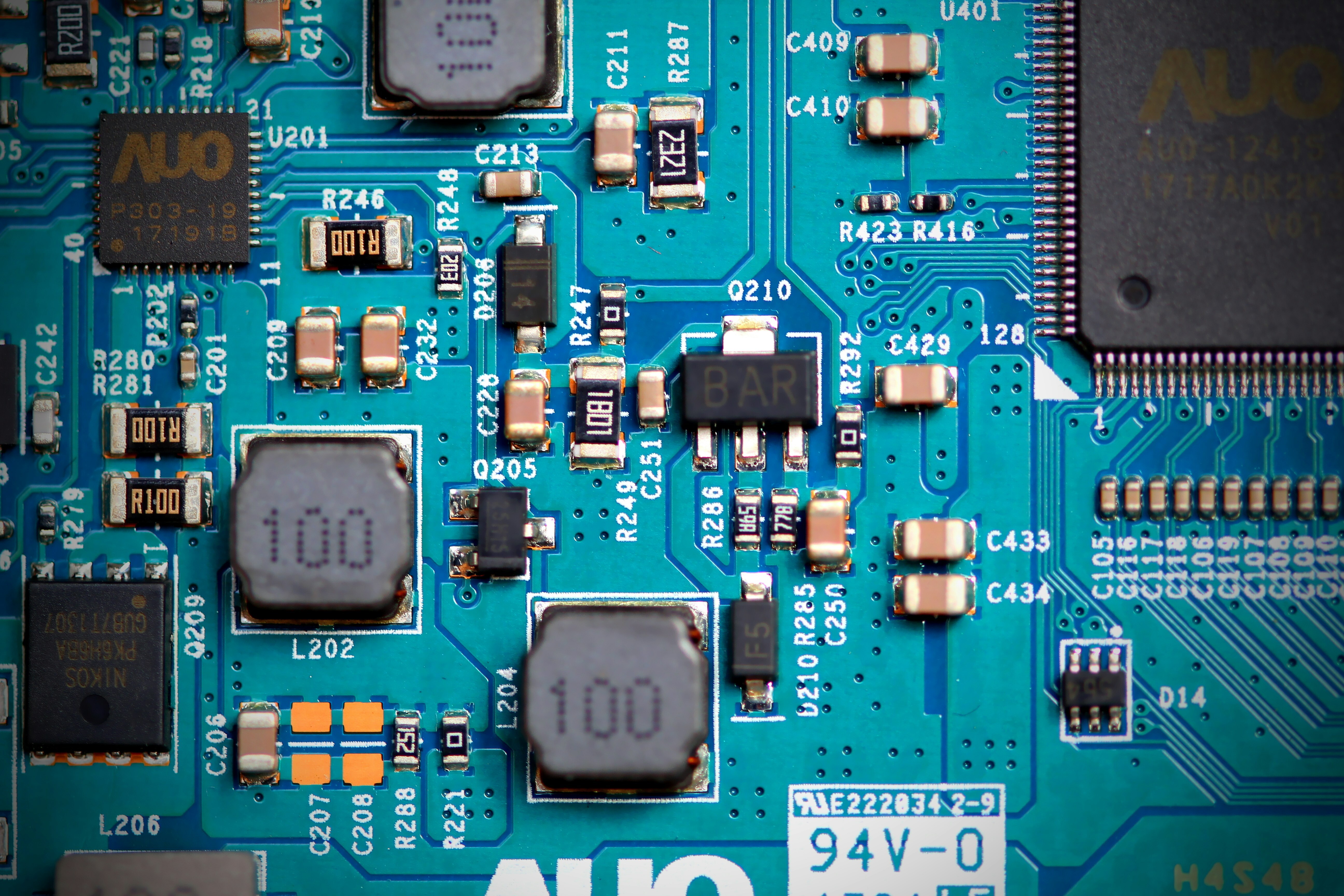
Laboratory Chemicals and Testing in the Semiconductor Industry
The semiconductor industry is essential to the global economy, powering everything from smartphones and computers to medical devices and automotive electronics. To ensure the precision, performance, and reliability of semiconductor components, laboratory testing and high-purity chemicals are indispensable throughout the manufacturing process. From wafer fabrication to packaging, a wide range of chemical processes is involved.
In this article, we explore the critical laboratory chemicals used in semiconductor manufacturing, the key testing processes, and how chemical distributors support semiconductor companies in maintaining product quality and operational efficiency.
What Is the Semiconductor Industry?
The semiconductor industry designs and manufactures semiconductors—materials with electrical conductivity between conductors (like metals) and insulators (like ceramics). These are foundational for integrated circuits (ICs) used in modern electronics. Semiconductor manufacturing involves complex processes such as:
-
Wafer fabrication
-
Etching
-
Doping
-
Packaging
-
Testing
Due to the microscopic scale of semiconductor components, laboratory chemicals are used to clean, etch, and process materials to achieve the desired characteristics of electrical conductivity.
Key Laboratory Testing and Chemicals in Semiconductor Manufacturing
1. Wafer Cleaning and Surface Preparation
Before any semiconductor device is fabricated, the wafer's surface must be cleaned of contaminants. This ensures the material can be precisely etched and doped to achieve the desired electronic properties.
Cleaning Methods:
-
Wet cleaning with chemicals such as hydrogen peroxide (H₂O₂), ammonium hydroxide (NH₄OH), and deionized water
-
Plasma cleaning for residue removal
Chemicals Used:
-
Acids: Hydrochloric acid (HCl), nitric acid (HNO₃)
-
Bases: Sodium hydroxide (NaOH), potassium hydroxide (KOH)
-
Solvents: Isopropyl alcohol (IPA), acetone
-
Oxidizing agents: Hydrogen peroxide (H₂O₂)
2. Etching and Pattern Transfer
Etching is the process by which specific patterns are transferred to the wafer’s surface, which is a critical step in the manufacturing of microchips. This process can be either wet etching or dry etching (plasma etching).
Wet Etching:
-
Involves the use of acidic or basic solutions to remove material from specific areas on the wafer.
Dry Etching:
-
Plasma or ionized gases are used to remove material from the wafer surface.
Chemicals and Gases for Etching:
-
Hydrofluoric acid (HF) – used in wet etching for oxide layers
-
Sulfuric acid (H₂SO₄) – for cleaning and etching
-
Chlorine-based gases (Cl₂), fluorine-based gases (CF₄) for dry etching
-
Plasma gases: Oxygen (O₂), argon (Ar), chlorine (Cl₂)
3. Doping (Ion Implantation)
Doping is the process of introducing impurities (dopants) into a semiconductor material to modify its electrical properties. The process is done through ion implantation, where ions are accelerated and implanted into the wafer.
Common Dopants:
-
Phosphorus (P), boron (B), arsenic (As) for n-type and p-type doping
Chemicals and Reagents:
-
Phosphorus oxychloride (POCl₃), diborane (B₂H₆) for dopant introduction
-
Solvents for cleaning after implantation
-
Gases for ion implantation: Argon (Ar), oxygen (O₂)
4. Chemical Mechanical Planarization (CMP)
CMP is a process used to flatten the surface of the wafer after multiple layers have been deposited or etched. It helps achieve planar surfaces and ensures uniform layer deposition, which is crucial for device performance.
Chemicals for CMP:
-
Slurry chemicals – cerium oxide (CeO₂) or aluminum oxide (Al₂O₃) in water for polishing
-
Oxidizing agents – hydrogen peroxide (H₂O₂) for oxidation
-
Acids – sulfuric acid (H₂SO₄) for cleaning post-polishing
5. Packaging and Soldering
Once semiconductor chips are fabricated, they need to be packaged and soldered to ensure they function correctly in electronic devices. Packaging is done by attaching the chip to a substrate and connecting it to external pins or leads.
Materials and Chemicals for Packaging:
-
Soldering flux – rosin-based, water-soluble, or no-clean fluxes
-
Epoxy resins – for chip encapsulation and bonding
-
Silver paste, gold, and copper for bonding wires and connections
Essential Chemicals for Semiconductor Manufacturing
| Chemical/Reagent | Purpose |
|---|---|
| Hydrogen Peroxide (H₂O₂) | Wafer cleaning, oxidation agent |
| Hydrochloric Acid (HCl) | Wafer cleaning and etching |
| Sulfuric Acid (H₂SO₄) | Cleaning and etching |
| Hydrofluoric Acid (HF) | Etching oxide layers and wafer surface preparation |
| Isopropyl Alcohol (IPA) | Cleaning and solvent for resist and surface prep |
| Argon (Ar) | Plasma etching and ion implantation |
| Phosphorus Oxychloride (POCl₃) | Dopant for n-type semiconductors |
Why Chemical Suppliers Are Crucial to the Semiconductor Industry
Semiconductor manufacturers rely heavily on high-purity chemicals to ensure the precision and quality of their components. Key requirements for these chemicals include:
-
Purity: Chemicals must be free of contaminants that could impact semiconductor performance.
-
Consistency: Chemical batches must be reproducible and meet stringent quality standards.
-
Regulatory Compliance: Chemicals must meet local and international standards, including REACH and GHS guidelines.
-
Availability: Quick delivery and reliable stock management to ensure production timelines are met.
At 949 Chemical, we supply semiconductor manufacturers across San Diego, Orange County, Los Angeles, and Santa Barbara with the high-quality chemicals and reagents required to maintain product integrity and precision throughout the semiconductor production process.

